AOP-A-010 is primarily composed of hydroxy silane. When spin-coated onto the substrate surface, its silanol groups (–Si–OH) react with hydroxyl groups (–OH) on the substrate, forming stable Si–O covalent bonds, as illustrated in Figure 1. This reaction replaces the original hydrophilic functional groups and results in the formation of an ultrathin (~15 nm) silane coupling layer. This layer significantly enhances the chemical adhesion between the photoresist and the substrate.
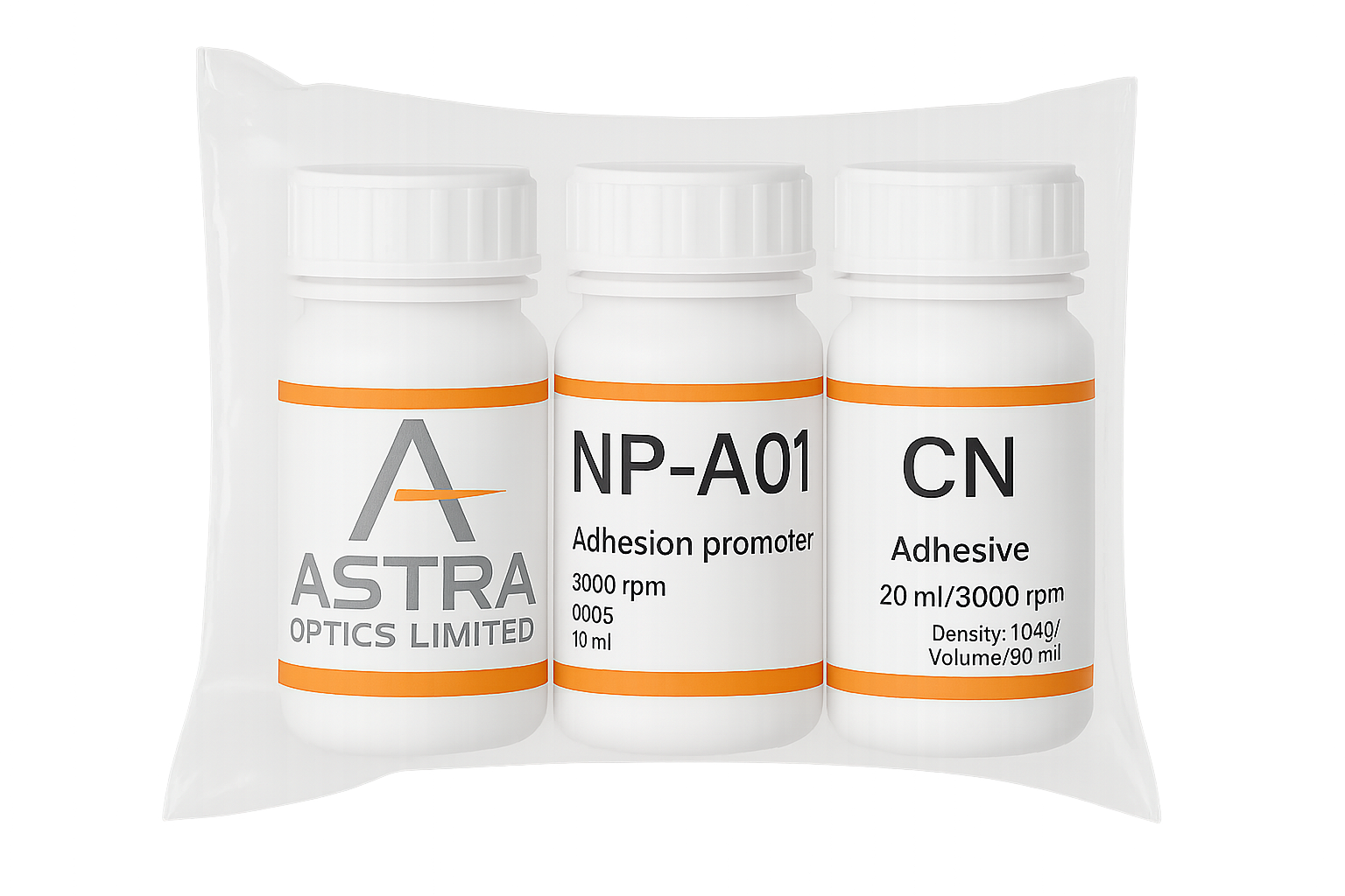
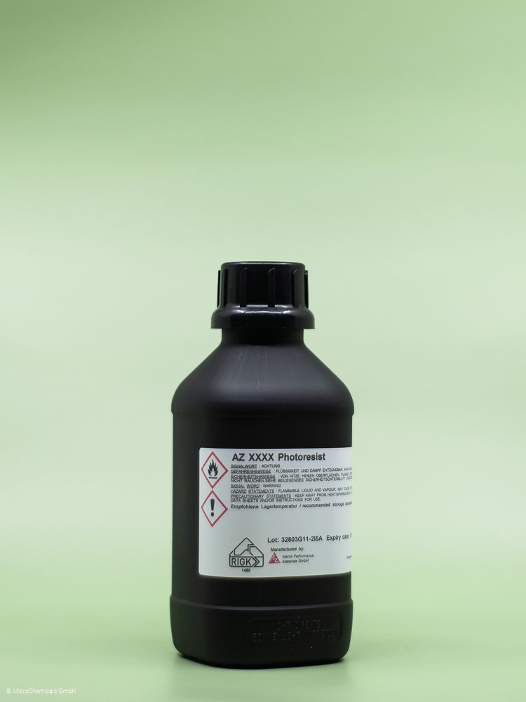
AOP-A-010 Adhesion Promoter
AOP-A-010 Adhesion Promoter
An advanced chemical solution with strong adhesion and low residue
AOP-A-010 is primarily composed of hydroxy silane. When spin-coated onto the substrate surface, its silanol groups (–Si–OH) react with hydroxyl groups (–OH) on the substrate, forming stable Si–O covalent bonds, as illustrated in Figure 1. This reaction replaces the original hydrophilic functional groups and results in the formation of an ultrathin (~15 nm) silane coupling layer. This layer significantly enhances the chemical adhesion between the photoresist and the substrate.
Product Advantages
Enhanced Adhesion
Forms stable Si–O covalent bonds that strongly anchor to the substrate surface, significantly enhancing photoresist adhesion.
Reduced Residue
Soluble in PGMEA developer, leaving no residue after development and ensuring a clean surface.
High Thermal Stability
After thermal annealing at 150–180 °C, the treated layer remains stable and does not interfere with subsequent processes.
Performance Validation
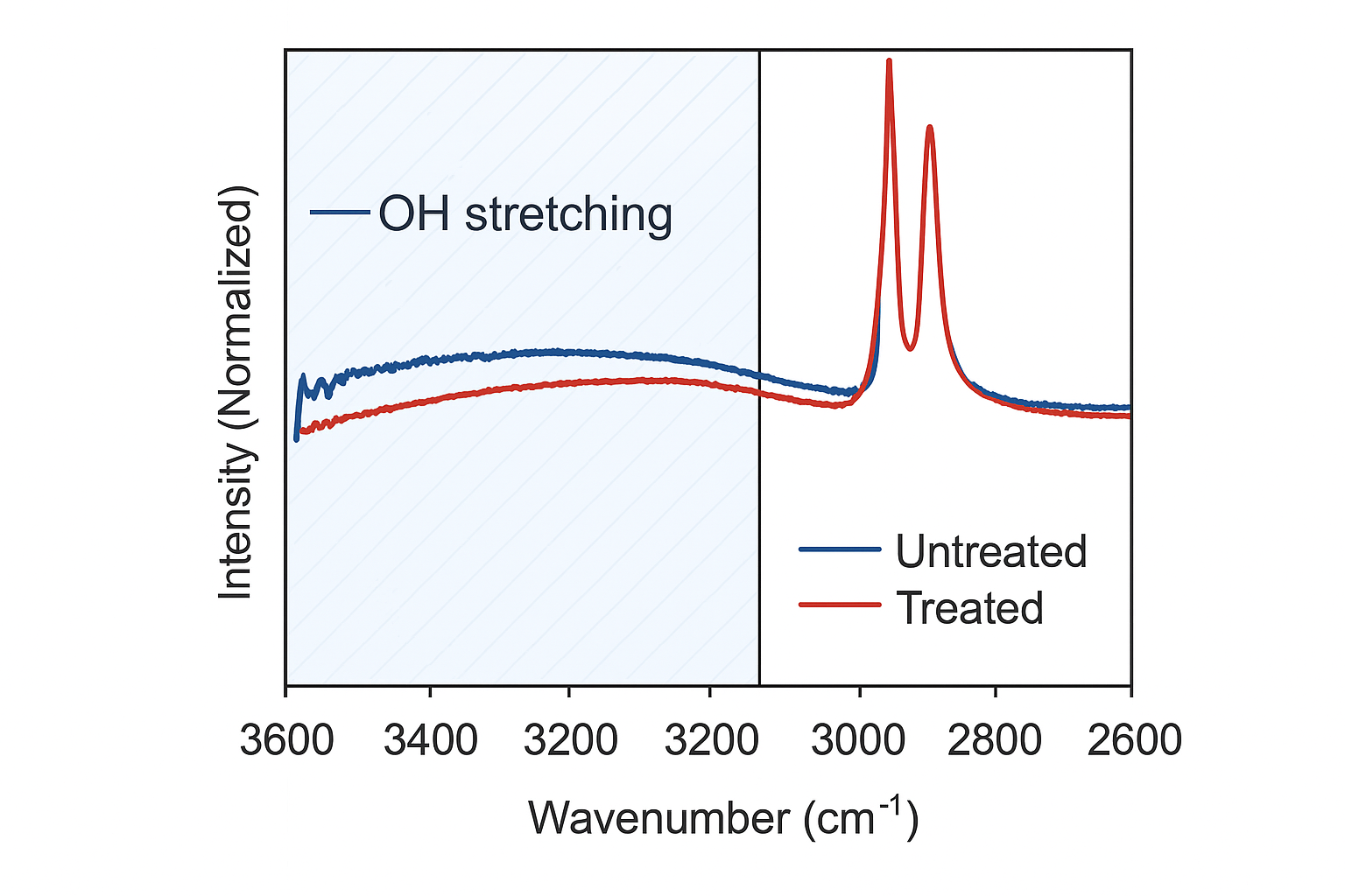
FTIR Analysis Results:
FTIR analysis indicates a distinct hydroxyl (–OH) absorption peak in the range of 3100–3600 cm⁻¹ before treatment. After treatment with AOP-A-010, the intensity of this hydroxyl peak is significantly reduced, indicating a decrease in surface-active hydroxyl groups and the successful formation of Si–O chemical bonds. This confirms a substantial enhancement in the adhesion between the photoresist and the substrate.
Quality Validation
The data has been validated through three rounds of in-house laboratory testing and is based on infrared spectroscopy analysis, ensuring authenticity and reliability.
During development, it is soluble in PGMEA, preventing residue that could affect subsequent processing.
Step 4
Market Analysis and Innovative Solutions for Semiconductor Lithography Adhesion Promoters
As semiconductor processes continue to scale down and become more refined, the adhesion between photoresists and substrates has emerged as a critical factor influencing the stability of micro/nanostructures and overall manufacturing yield. Adhesion promoters, as key materials addressing this challenge, play a decisive role in determining both the success of the lithography process and the long-term reliability of the final devices.
This report presents a comprehensive comparative analysis of mainstream adhesion promoter products in the market, with a special focus on our innovative solution — AOP-A-010. By overcoming the limitations of conventional technologies, AOP-A-010 delivers exceptional performance tailored for next-generation lithography applications.
Conventional Products
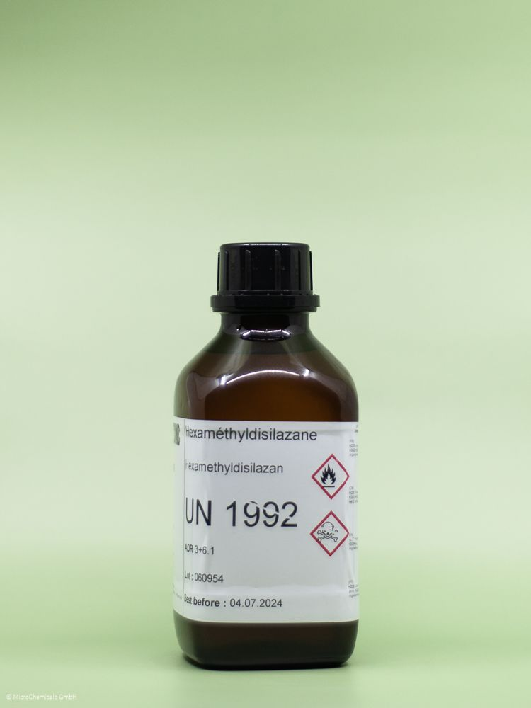
HMDS (Hexameth
yldisilazane)
HMDS (Hexamethyldisilazane)
Working Mechanism:HMDS reacts with silicon atoms on oxygen-free surfaces and with oxygen atoms on oxidized surfaces, releasing ammonia gas as a byproduct.
Key Characteristics:Its non-polar methyl groups isolate the substrate surface, forming a hydrophobic layer that enhances photoresist wetting and adhesion.
Usage Method:Requires a dedicated vapor priming system and must be applied under heating conditions between 75–120 °C.
Limitations:Complex handling and equipment requirements,Chemically toxic,Suitable only for positive photoresists
Ti Prime
Working Mechanism:Under thermal activation, titanium ions bond with hydroxyl groups, resulting in a substrate surface with reduced hydroxyl content.
Key Characteristics:Spin-coating-based process that effectively improves adhesion on silicon or glass substrates.
Usage Method:Spin coat at 2000–4000 rpm for 20 seconds, followed by:Hot plate baking at 120 °C for 2 minutes, or,Oven baking at 130 °C for 10 minutes
Limitations:Still exhibits mild toxicity,Compatible only with positive photoresists
AR 300-80
AR 300-80
Working Mechanism:Forms a ~15 nm polymer film that integrates seamlessly with the subsequent photoresist layer.
Key Characteristics:Easy to apply,Non-toxic,Removable with organic solvents without compromising adhesion performance
Usage Method:Spin coat at 4000 rpm,Bake on hot plate at 180 °C for 2 minutes or oven bake for 25 minutes
Improved Version:AR 300-80 new is suitable for temperature-sensitive substrates and requires only 60 °C baking.
Limitations:Not compatible with drop-casting processes in two-photon lithography (TPL),May introduce bubbles at the interface, potentially causing structural defects
Chaonai Innovative Products
AOP -A-010
AOP -A-010
Working Mechanism:Based on AR 300-80 technology, this formulation incorporates a proprietary surface energy suppressant to enhance interfacial performance.
Key Advantages:
Unique Bubble Suppression Technology :Effectively addresses bubble formation during drop-casting in two-photon lithography (TPL) processes.
Easy Operation :Requires only hot plate baking—no need for complex equipment.
Broad Compatibility :Suitable for both positive and negative photoresists.
Environmentally Friendly :Completely non-toxic and aligned with modern green semiconductor manufacturing standards.